Today's quantum systems are bottlenecked by their classical control. Coaxial cables, room-temperature electronics, and fan-out wiring don't scale past a few hundred qubits. TYNANA replaces that stack with photonic signal distribution above the fridge and a programmable cryo-CMOS layer at base temperature.
Every superconducting or solid-state qubit needs precisely timed microwave pulses for gates and readout. The way the industry delivers those pulses today doesn't survive past a few hundred channels — and that's the wall every roadmap hits.
Modern dilution refrigerators are filled with stainless and copper coaxial cables — one or more per qubit, every line carrying heat down to the mixing chamber. Past a few hundred qubits there is literally no room left and the thermal load exceeds the cooling budget.
Each pulse channel today sits on a benchtop AWG and amplifier dissipating tens of watts. Multiply that by 1,000+ channels and the control rack alone draws more than the rest of the lab. That doesn't scale to fault-tolerant qubit counts.
Real-time error correction needs measurement-to-correction latency under a microsecond. With control electronics three meters away at room temperature, the speed-of-light round-trip alone eats most of the budget — long before the FPGA even decides what to do.
RF control is programmable but doesn't scale. Pure photonic links scale distribution but lose local programmability. TYNANA combines both — using each technology where it actually wins.
Encode pulse waveforms as modulated optical signals at room temperature, then carry them down the fridge over a single fiber bundle. Wavelength-division multiplexing puts dozens of channels on one fiber.
A standard 22nm FD-SOI chip running at 4 K decodes incoming optical pulses, drives gate waveforms, and clocks readout — all within a few centimeters of the qubits. Per-qubit timing and feedback stay programmable.
Photonic and electronic die are bonded with μBumps and a passive fiber array, forming one cryogenic module. No long RF runs inside the fridge, no hand-tuned cabling — just a programmable control board sitting next to the qubits.
The TYNANA stack is built around a vertically-integrated module. The upper layer is a photonic PIC that fans out incoming optical pulses across qubit lines. The lower layer is a cryo-CMOS controller that converts those pulses into precisely-timed waveforms and feeds back measurement results.
Both die are co-packaged with a passive fiber array at the bond interface. The result: one connector going into the fridge instead of hundreds.
Photonic integrated circuits in silicon nitride and III-V compound semiconductors carry pulse waveforms from room-temperature electronics down to the fridge as modulated light. One fiber bundle replaces hundreds of coaxial lines; wavelength multiplexing layers eight channels onto each fiber.
Inside the cryogenic stage, an arrayed-waveguide grating splits the incoming light by wavelength, photodiodes recover the original pulse shape, and the signal hands off to the cryo-CMOS controller through short on-package traces.
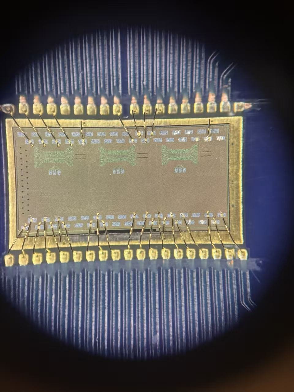
Standard CMOS still works at 4 K — at the cost of a small shift in transistor behavior — and that's the trick TYNANA's controller exploits. Built in 22nm FD-SOI, the cryo-CMOS die decodes incoming pulses, drives gate waveforms through low-noise DACs, and pipes measurement results back through an ADC and amplifier chain.
Because logic and gating sit a few centimeters from the qubits, real-time correction loops can close in under a microsecond — which is what fault-tolerant operation actually needs.
The photonic and electronic layers are joined into a single cryogenic module by a μBump array carrying the recovered electrical signal and a passive fiber array carrying the optical input. No wire bonds, no long RF runs inside the fridge — just one package the customer drops into their existing dilution refrigerator.
This is what makes the architecture deployable instead of a research curiosity: standard packaging techniques borrowed from silicon photonics for the bond, standard mounting for the qubit-side connectors, and a host-side FPGA over a single fiber bundle.
This is the cryo-CMOS controller after wire-bonding — etched logic and analog blocks on the die surface, gold ribbon bonds connecting to the package frame, and the supporting routing pattern visible on the underlying carrier. Every visible feature was placed on a foundry-qualified PDK.
Each existing approach to qubit control gets one thing right and another thing wrong. TYNANA picks the right tool for each layer instead of forcing one technology to do both jobs.
| Property | Room-temp RF (today's stack) |
All-photonic (research) |
TYNANA Hybrid |
|---|---|---|---|
| Wiring per qubit | 1+ coax line | Shared fiber | Shared fiber bundle |
| Power per channel | Tens of W | mW class | mW class @ fridge |
| Programmable timing | Yes (FPGA) | Limited / fixed | Yes — local cryo-CMOS |
| Real-time feedback | µs scale, distance limited | Hard — no local logic | <1 µs in-fridge |
| Scaling ceiling | Hundreds of qubits | Thousands, but rigid | Thousands, programmable |
| Manufacturable today | Yes | Custom only | Standard MPW + foundry CMOS |
TYNANA was incorporated in 2026. The current focus is a small-channel hybrid prototype that closes the loop end-to-end at base temperature. Each generation widens the channel count and tightens the integration.
8–10 channel hybrid module. Tape-out on AIM Photonics MPW (TYN-P) and GF22FDX (TYN-E). Validate end-to-end pulse delivery and readback at 4 K.
Bench demonstration with a partner qubit lab. Closed-loop feedback at <1 µs latency on superconducting transmon test devices.
First customer-deployable cryogenic control board. Standard mount in commercial dilution refrigerators. Wavelength count up to 16 per fiber.
Modular 1k-channel deployments aimed at logical-qubit demonstrations. Co-design with qubit hardware partners on per-platform variants.
TYNANA LLC was incorporated in 2026. We're a two-person founding team, pre-launch, with no patents granted yet. The architecture, channel counts and process choices on this page reflect our current technical plan — not shipping product. We share this roadmap because customers and collaborators deserve the real picture, not a polished press release.
If you're running a qubit lab, building a fault-tolerant roadmap, or working on cryogenic packaging — we want to hear from you. The earliest module slots are reserved for partners shaping the spec.