Technology Use Cases Resources About Careers Foundry Contact Us
About TYNANA

The Control Stack
for Useful
Quantum Computing.

Tynana LLC is a 2026-incorporated, two-founder quantum control infrastructure startup. We build the photonic + cryo-CMOS layer that lets quantum processors actually scale — not the qubits themselves.

Our Mission

Make the control plane the easy part.

"Every quantum platform — superconducting, ion-trap, spin, neutral-atom — runs into the same wall: too much room-temperature wiring, too much heat, too much latency. We remove that wall."

Tynana LLC was founded in 2026 by Bowen Liu (CTO), a mechanical engineer, and Peter Zhang (CEO), an attorney. We are pre-revenue, pre-product, and intentionally narrow: a single architectural bet that hybrid photonic distribution combined with cryo-CMOS local control is the right way to deliver pulses to thousands of qubits without melting the fridge or the cable budget.

Architecture-First

We do not build qubits. We build the photonic + cryo-CMOS control layer that sits between the room-temperature host and any qubit modality.

Built on Real Tapeouts

Two chip tapeouts in six weeks across AIM Photonics (SiN) and GlobalFoundries 22nm FD-SOI (GF45SPCLO). No paper architectures.

Modality-Agnostic

Our hybrid stack targets superconducting transmons first, but the same primitives apply to trapped ions, neutral atoms, and silicon-spin qubits.

Partnership Pipeline

Pre-launch in 2026. Co-design conversations with academic groups and quantum-hardware teams; foundry collaborations with AIM Photonics and GF.

Our Approach

The control plane is the bottleneck — so we redesigned it.

Most quantum-hardware companies are racing to add qubits. The wall they keep hitting is not qubits — it is the dense thicket of coax, attenuators, isolators, and amplifiers required to drive and read those qubits. Tynana attacks that wall directly with a hybrid photonic + cryo-CMOS architecture that replaces bulk RF cabling with a handful of optical fibers and moves last-millimeter pulse generation onto a CMOS chip a few millimeters from the qubit plane.

01 — Layer

Photonic Distribution

Pulse parameters travel from a room-temperature FPGA host as DWDM-encoded light on a single fiber. SiN waveguides at 4K demultiplex the channels and hand them to the electronic die.

02 — Layer

Cryo-CMOS Local Control

A 22nm FD-SOI chip running below 4K decodes incoming bits, generates microwave pulses, captures readout signals, and runs sub-microsecond feedback loops next to the qubits.

03 — Layer

Hybrid Bonded Module

The photonic and electronic dies are µbump-bonded at the package level — short electrical paths, no fragile fly-leads, manufacturable on existing tooling.

04 — Outcome

~10× Wiring Reduction (Target)

An 8-channel prototype targets roughly an order-of-magnitude reduction in coax cables compared to a conventional control rack at the same channel count.

05 — Outcome

<1µs Feedback Latency

Local control means measurement-conditioned operations close at the chip rather than at the rack. That is the regime where useful error correction lives.

06 — Foundation

Foundry-Native

Built on AIM Photonics SiN PDK and GlobalFoundries 22nm FD-SOI (GF45SPCLO). Both processes are commercially available — no exotic fabrication required.

Real Hardware

Architecture meets silicon.

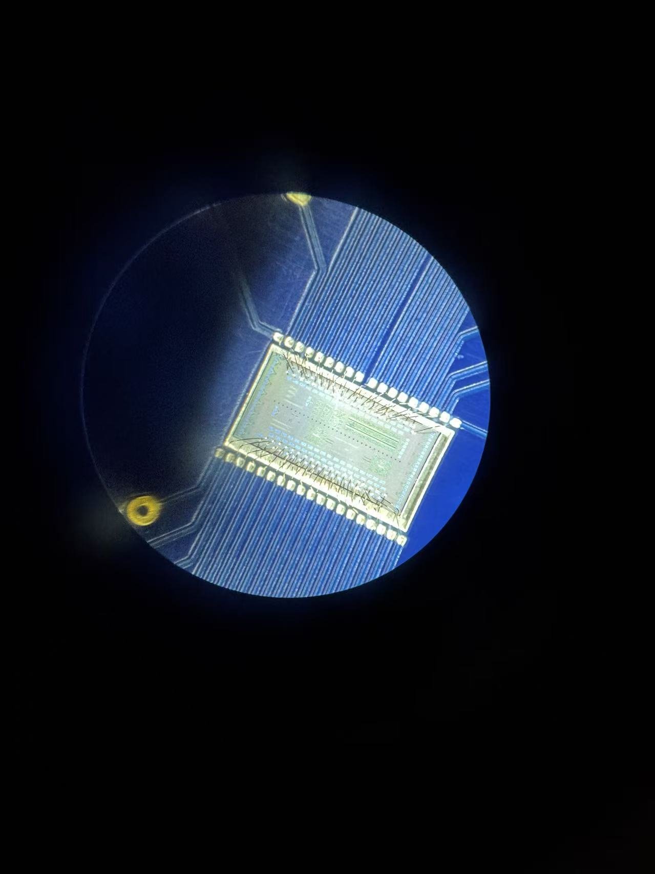
The story Tynana tells is not a paper architecture. The cryo-CMOS controller die is wire-bonded onto a custom routing PCB, with the trace network fanning out to test instrumentation. This is the level of physical readiness the architecture has reached today — not a render, an actual board on the bench.

Wider macro perspective of a wire-bonded microchip mounted on a blue PCB, with the parallel trace network fanning outward toward gold fiducial markers.
Cryo-CMOS controller — chip + carrier board Wire-bonded die on routing PCB with fan-out trace network. The exposed trace pattern routes pulse drive, readout, and supply lines to the chip pads under test. Hardware · GF 22nm FD-SOI · Carrier-bonded
Leadership

The team behind the technology

TYNANA is led by technologists and operators who combine deep quantum physics expertise with the commercial instincts to build a lasting company.

Photo coming soon
Replace with portrait
Peter Zhang
Co-Founder & Chief Executive Officer

Peter leads commercial strategy, partnerships, and operations at Tynana. He owns customer discovery with quantum-hardware groups and runs fundraising, hiring, and the build-out of foundry and supplier relationships.

  • Co-founder, 30% equity holder
  • Customer development across superconducting, ion-trap, and spin-qubit labs
  • Operations, recruiting, and investor relations
  • PeterZhang@tynana.com
LinkedIn
Photo coming soon
Replace with portrait
Bowen Liu
Co-Founder & Chief Technology Officer

Bowen is the technical architect behind Tynana's hybrid photonic + cryo-CMOS control stack. He drove two foundry tapeouts in six weeks — one on AIM Photonics SiN, one on GlobalFoundries 22nm FD-SOI — and designs both the photonic integrated circuit and the cryo-CMOS ASIC.

  • Co-founder, 70% equity holder
  • PhD candidate, Physics — Rensselaer Polytechnic Institute (exp. 2029)
  • MS, Electrical Engineering — Columbia University (2024)
  • BS, Electrical Engineering & Physics — RPI (2022)
  • Tapeouts: GF 22nm FD-SOI (GF45SPCLO) & AIM Photonics SiN PDK
  • BowenLiu@tynana.com
LinkedIn